
This guide is all about how to prevent those delays. It is not just about a design. It is about a strategy for product development that is built on structured, manufacturable PCB design guidelines to maintain a faster, more predictable, and more cost-effective launch.
Table of Contents
How Structured PCB Design Guidelines Accelerate Your Launch
A product launch can be completely derailed, not by a single big setback, but by a thousand tiny, preventable design flaws. These “paper cuts” in your PCB design guidelines are flaws that look perfect in a CAD file but cause massive, costly delays on the factory floor.
This guide is all about how to prevent those delays. It is not just about a design. It is about a strategy for product development that is built on structured, manufacturable PCB design guidelines to maintain a faster, more predictable, and more cost-effective launch.

A complex electronic sub-assembly unit shown in mid-production. PCB design guidelines directly impact the final box build, as component placement and connector choices must be optimized for integration with wiring harnesses, power supplies, and enclosures.
What are the Core Principles of an On-time PCB Design?
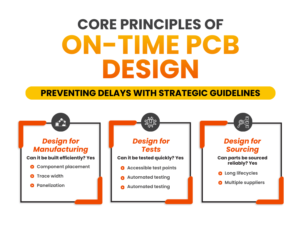
To prevent delays, a design must be optimized for the real world, not just for a schematic. This means your PCB design guidelines must be built on three core, timesaving principles:
- First is Design for Manufacturing (DFM). This principle asks, “Can it be built efficiently and repeatably?” This considers factors like component placement, trace width, and panelization to speed up automated assembly.
- Second is Design for Test (DFT). This asks, “Can it be tested quickly and accurately?” It involves adding accessible test points and designing the board so automated testing equipment can validate every unit without costly manual checks.
- Third is Design for Sourcing (DFS), which covers the question “Can the parts be sourced reliably and without delays?” This strategic part of your PCB design guidelines involves selecting components with long lifecycles and multiple suppliers. This simple step can prevent a single “out of stock” part from halting your entire production line.
What are the Top PCB Design Challenges That Cause Launch Delays?
The most frustrating delays often stem from a disconnect between the design engineer and the manufacturing floor. This is especially true for complex or miniaturized devices. Common problems in the initial PCB assembly and design phase include:
- Poor Component Selection: Choosing components that are near end-of-life (EOL) or are single-sourced. A sudden supply chain shortage can force a complete and costly redesign, adding months to your timeline.
- Suboptimal Layout: Placing components too close together or too near the board’s edge. This can make the contract manufacturing electronic assembly process difficult or impossible for automated pick-and-place machines, forcing slow and expensive manual rework.
- Ignoring System-Level Integration: Designing the PCB in a vacuum. A board that works perfectly on its own but does not fit the enclosure, overheats, or has connectors that clash with wiring harnesses is a failed design. This failure will likely be caught at the final, most expensive stage.

Two engineers collaborate on a design, illustrating the critical importance of early DFM (Design for Manufacturability) review. This partnership between design and manufacturing experts is important for developing PCB design guidelines that prevent costly production delays.
How Does DFM Software Prevent These Manufacturing Delays?
Design for Manufacturability (DFM) analysis is the formal process of using specialized software to analyze a PCB design specifically for its manufacturability. It is the practical, automated application of good PCB design guidelines.
This software acts as an expert reviewer. It catches thousands of technical errors that cause delays, such as:
- Traces and pads that are too close, risking electrical shorts.
- Incorrect land patterns that would lead to weak or failed solder joints.
- Acid traps or solder mask slivers that reduce production yield.
A DFM check is the single best way to catch and fix these problems before they become physical, costly delays. When integrated into prototype development services, it helps confirm that your design is viable.
Why DFM Requires an Experienced Manufacturing Partner
While DFM software is powerful, it is not a complete solution. It can catch technical rule violations, but it cannot provide strategic advice on the manufacturing process.
An automated check cannot tell you that a technically correct component is notoriously difficult to source. It also cannot tell you that by slightly moving a mounting hole, you could make the final assembly 30% faster.
This is where early collaboration with a contract manufacturer in the USA is essential. By reviewing your design, they provide invaluable, real-world manufacturing support services that no software can match. This collaborative human insight is the most advanced part of your PCB design guidelines.
The Role of PCB Design Guidelines in Box Build for Preventing Failures
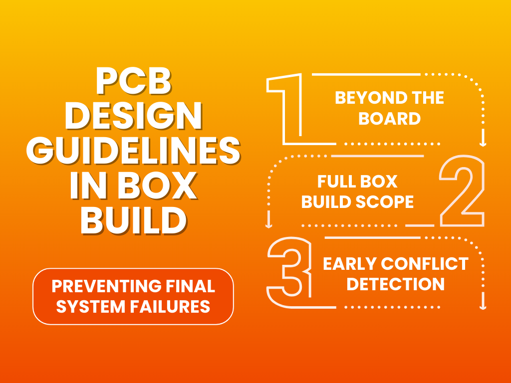
The most costly delay happens at the very end. The PCB is perfect, but it does not work as part of the final system. This is why your PCB design guidelines must extend beyond the board and encompass the entire product. This is the domain of box build printed circuit board assembly services.
A manufacturing partner who understands the full box build assembly services (the enclosure, wiring, power supply, and user interface) can identify system-level conflicts early in the design phase. They will spot issues like port misalignment, thermal “hot spots,” or connector mismatches. This prevents the final-stage failures that are the most devastating to a launch schedule.
How Can I Protect My Circuit Design (IP) During Production?
While you are designing to prevent manufacturing delays, a competitor stealing your design can delay or destroy your market advantage. Protecting your IP is a critical part of your production strategy and your PCB design guidelines.
Beyond erasing chip details, an IP protection strategy includes two key parts:
- Technical Obfuscation, like using multi-layer boards to bury critical traces in inner layers or covering key areas of the board with opaque potting epoxy.
- Strategic Partnership with a contract manufacturer in the USA who is bound by U.S. intellectual property laws and a comprehensive non-disclosure agreement.
Design Products for Launch, Not Just for Function
Poor PCB design guidelines are often a major contributor to preventable product launch delays. By shifting your focus from a design that merely “works” to one that is manufacturable, testable, and sourced decisively, you are creating a strategy for product development that is built for speed and reliability.
The most effective way to do this is to partner with a box build custom manufacturing service that sees the full picture. You need a partner who understands the entire process from the first prototype to the final shipment.
MFG One provides box build custom manufacturing services for clients across the United States, Canada, the United Kingdom, Mexico, and beyond. Contact us today to align your design with your launch goals.